








Photonic Chips Gain Momentum in Europe
Europe is poised to seize an opportunity that could revolutionize the computer chip industry, according to Ton van Mol, a researcher at the Dutch research institute TNO.
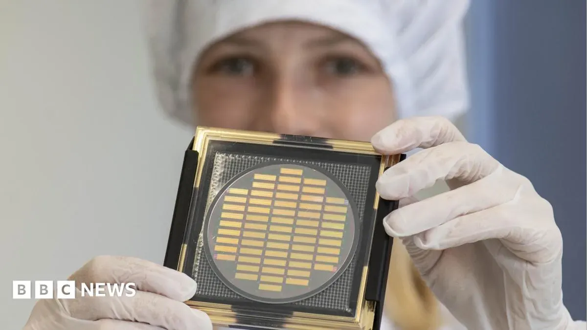
Europe is poised to seize an opportunity that could revolutionize the computer chip industry, according to Ton van Mol, a researcher at the Dutch research institute TNO.
TNO and other key players in Europe are betting big on photonic chips, which use light instead of electricity to process data. The technology has the potential to outperform traditional electrical chips by being faster, using less energy, and generating less heat.
The current state of computer chip production relies heavily on electrical signals, with each microchip containing billions of transistors and measuring in nanometres. This process is a legacy of the 1970s, when electrical chips first began to dominate the industry.
Van Mol compares the photonic chip technology to where electronic chips were about 40 or 50 years ago, suggesting that it has significant potential for growth and development. He believes that Europe can leverage this emerging field to regain leadership in a key future technology area.
The European Union has already committed €400m to a project called PIX Europe, which aims to establish the continent as a global leader in photonic integrated chip technology.
The European Union has identified photonic integrated chip technology as a key area for investment and innovation. According to van Mol, who is leading a crucial part of the programme, Europe needs to have its own manufacturing capabilities in-house. This means moving away from relying on other countries like the US or China for chip production, which he describes as "not wise.
To address this issue, the European Chips Act was introduced, aiming to bring cutting-edge technology from laboratories into industrial-scale manufacturing. One of the key components of the act is the establishment of pilot lines that can produce photonic chips on a larger scale.
The current method of producing electronic and photonic chips involves creating wafers with hundreds of individual chips. However, factories equipped with machines capable of handling bigger wafers can significantly increase production efficiency.
Van Mol's team is working towards scaling up production from four-inch to six-inch wafers, which he believes will be a major step forward in the field of photonics worldwide. This move involves transitioning from current manufacturing methods to more advanced technology.
A 10,000 sq m factory is currently under construction on the High Tech Campus in Eindhoven, the Netherlands, with the aim of producing six-inch indium phosphide wafers by 2030. According to van Mol, this development will be a significant milestone not only for Europe but also globally.
The plan to establish a pilot line for commercial production of photonic chips is set to be a significant milestone in 2030. The line will feature ASML products at its core, which are currently the only machines capable of making the most sophisticated semiconductors worldwide. This strategic placement is no coincidence, given that the project is based near ASML's headquarters in Eindhoven.
The production method for photonic chips bears a striking resemblance to traditional semiconductor technology. According to van Mol, wafers and high-end clean rooms are used, mirroring the equipment employed in electrical or electronic chip manufacturing. This similarity will likely facilitate the transition from research to industrial-scale production.
ASML is keen to explore the opportunities presented by photonics technology. The company recognizes Europe's strong position in photonic research and sees the next challenge as translating innovations into large-scale manufacturing. ASML's expertise has helped establish a network of companies and institutions focused on semiconductor technology in the Eindhoven region, serving as a model for Europe's efforts.
The Netherlands-based tech giant is uniquely positioned to drive this transition forward. With its machines at the heart of the pilot line, ASML will play a pivotal role in commercializing photonic chip production. This collaboration between industry leaders and research institutions has the potential to propel Europe to the forefront of photonics innovation.
ASML's head of EU/US Customer Team, Stanislas Baron, emphasizes the need for translating innovations into industrial-scale manufacturing. He highlights Europe's strong position in photonics research, but notes that this is only half the battle, turning those discoveries into a commercial reality will be crucial to success.
The Eindhoven project has garnered significant backing from industry experts, including former ASML chief executive Peter Wennink, who authored a report on the potential of photonics to drive economic growth. The report, titled The Roadmap to Future Prosperity, highlighted the market's expected 10-20 fold growth in the next decade.
Wennink has expressed his support for the Eindhoven project, describing it as a crucial launchpad for Europe's future digital economy. By investing in scalable production capacity, the continent can create an ecosystem that shapes global technological direction, he emphasized. According to Wennink, this investment will be instrumental in propelling Europe forward in the photonics industry.
The European Union is not alone in recognizing the potential of photonics to drive economic growth and innovation. In June, US-based Coherent announced a significant expansion of its production capacity with the launch of a six-inch indium phosphide manufacturing platform at its Texas facility. This development has been backed by major players such as Nvidia and received $50 million in public funding under the US Chips Act.
The rapid pace of advancements in photonics is evident in this expansion, which underscores the critical role that photonic chips will play in AI and technological development moving forward. As the global market continues to evolve, Europe's bid to establish itself as a leader in photonic chip production becomes increasingly urgent and strategic.
Industry experts like Joris Teer of the European Institute for Security Studies believe that this approach makes sense within a globalized economy. By prioritizing investment in photonics research and development, Europe can ensure its continued relevance and influence in the technology sector.
The European continent has a unique opportunity to take the lead in photonic chip development, which could have significant implications for future advancements in artificial intelligence and data storage.
The region's high energy costs and skilled workforce shortages make it challenging to compete with other major players in the industry, but experts say that by prioritizing investment in photonics research and development, Europe can ensure its continued relevance and influence.
Ton van Mol of TNO emphasizes that their goal is not to develop a product for the market, but rather to establish a foundry model" where multiple companies can design and build chips without having to invest heavily in production facilities. This approach has proven successful at scale with Taiwanese-based giant TSMC.
The Eindhoven project will provide a pilot production line that can be used by businesses across Europe and beyond, helping the industry to scale up and overcome production challenges. By easing these hurdles, van Mol believes that photonic chips can move from specialized areas like data centers and Lidar sensor technology into more mainstream applications like smartphones and laptops.
The ultimate goal is to drive innovation in areas such as medical scanners and 6G communications by making photonic chip technology more accessible and affordable for industry leaders.
Europe aims to capitalize on emerging photonic chip technology by establishing its own manufacturing capabilities, a strategic move that could position the region as a leader in data and telecom infrastructure.
By making these advanced chips more accessible and affordable for industry leaders, Europe hopes to drive innovation in cutting-edge fields like medical scanners and 6G communications.
Facts based on reporting originally published by BBC News Technology.
You may republish this story, in full or in part, if you credit Noti Group and link to it (licence CC BY 4.0). Photos are not included.